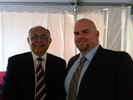
Today is the day of much anticipated July 24th groundbreaking for Fab 2 in Saratoga County, NY! Once constructed, analysts expect Fab 2 to be the worlds most advanced semiconductor foundry. Its construction represents more than three-years of careful planning and collaboration and an investment of roughly $4.2B Our friend Ian McNaughton from AMD is at the groundbreaking ceremony this morning and sent us this picture of himself with GlobalFoundries Chairman – Hector Ruiz. It looks like some gold plated shovels will be in the ground very soon!

The technology in Fab 2 will be absolutely state of the art. Our current plan is to ramp it on 28nm technology in 2H 2012 and then make a quick transition to 22nm, in a similar fashion to what we did with Fab 36 for AMD in Dresden. Ramping on a mature technology generation reduces significant risk in bringing a new fab successfully online and into production. Of course Fab 2 will also come stacked with the latest generation of our patented APM software to ensure maximum automation, control and predictability in rapidly ramping production for our customers at mature yield.
